FR4 Propagation Delay Calculator
Estimate FR4 trace delay from length, Dk range, frequency dispersion, routing style, rise time, vias, and skew budget.
| FR4 Dk at 1 GHz | Adjusted Dk | Effective Dk | Delay rate | Speed |
|---|---|---|---|---|
| 4.0 | 3.95 | 3.05 | 148 ps/in | 6.8 in/ns |
| FR4 PCB preset | Typical Dk range | Loss/dispersion note | Good fit |
|---|---|---|---|
| Standard FR4 core | 4.10 to 4.70 | Normal Dk drift | General logic, MCU, low GHz |
| High-Tg FR4 | 4.05 to 4.55 | Stable assembly process | Dense boards, lead-free reflow |
| Low-loss FR4 | 3.65 to 4.05 | Lower dispersion | PCIe, USB, SATA planning |
| Mid-loss FR4 | 3.85 to 4.35 | Moderate high-speed drift | Cost-sensitive serial links |
| Lead-free assembly FR4 | 4.15 to 4.65 | Robust thermal cycle | Industrial controller boards |
| Thin prepreg FR4 | 3.95 to 4.45 | Geometry sensitive | Fine-pitch escape routing |
| Backplane FR4 | 3.75 to 4.25 | Controlled long traces | Connectors and card cages |
| Halogen-free FR4 | 4.00 to 4.60 | Vendor dependent | Compliance-driven designs |
| Prototype FR4 | 4.20 to 4.80 | Wide tolerance | Early home lab boards |
| Tight-Dk FR4 | 3.95 to 4.15 | Narrow tolerance | Timing-sensitive routes |
| Routing model | Field location | Typical FR4 ps/in | Design note |
|---|---|---|---|
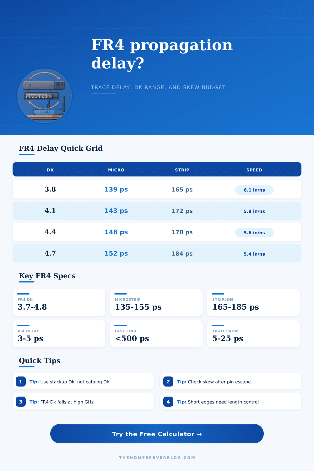
| Outer-layer microstrip | Air plus FR4 | 135 to 155 | Fastest common FR4 routing style |
| Outer coplanar microstrip | Air, FR4, side ground | 138 to 160 | Ground pour changes effective Dk |
| Embedded microstrip | Solder mask/prepreg cover | 150 to 170 | Between microstrip and stripline |
| Inner-layer stripline | Mostly FR4 | 165 to 185 | Slower but shielded and repeatable |
| Interface example | Common FR4 concern | Planning skew | Calculator use |
|---|---|---|---|
| PCIe / USB / SATA pairs | In-pair skew | 5 to 15 ps | Check length delta and via imbalance |
| DDR byte lane | DQS to DQ timing | 10 to 25 ps | Use stripline or exact stackup Dk |
| RGMII and source sync | Clock-to-data offset | 50 to 150 ps | Compare delay against timing budget |
| Low-speed control nets | Electrically long traces | 200 ps+ | Use rise-time fraction length |
I am sure you’ve all done this, where a schematic looks great on paper but fails in practice due to time issues. That is what happens when you route a high-speed interface. You connect the copper, match your impedance, but then the data comes too late or out-of-phase. That’s not magic. What usually happens is you didn’t properly take into account the fact that electricity travel very slowly inside fiberglass. Even though the speed of light in a vacuum is fast, it greatly slows as it passes through the molecular makeup of FR4 material. Managing amount of lag that accumulates across inches of trace is less about raw speed and more about understanding propagation delay.
By plugging your stack up into the calculator (above) we do all of the math so you don’t have to guess how much slower your stripline will be than your microstrip. By far most designers takes a value based off the chart for their dielectric constant and call it a day. Four point something is typical. They presume the board house nails the number dead-on. This is dangerous thinking.
Why Your Fast Signals Are Slow
A printed circuit board isn’t made out of uniform material called FR4. It’s a woven glass matrix impregnated with resin. The ratio of epoxy to glass vary depending on who makes it, where they make it, the weave pattern, and the press cycle. Using the nominal value listed in catalog will get you a timing budget. However, it ignores the tolerance band that determines if your signal is actualy going to meet the setup time.
Then there’s dispersion: As frequency rises, the effective dielectric constant of FR4 decreases slightly. In analog terms it’s a small effect, but if you’re trying to line up edges in tens of picoseconds it matters. This happens because a high-frequency part of a signal travels faster then a low-frequency part of that same signal. The tool allows you to enter the operating frequency and will adjust delay rate based on that. If you use data sheet values measured at one gigahertz but operate at a higher frequency, you’ll under-estimate the trace length necessary to achieve both impedance matching and skew control.
But what’s the deal with the delay? Well, you only care about the delay if the rise time is such that the signal travels far enough to matter. For example, a signal with a rise time of only a few nanoseconds must travel a long distance before it start acting like a transmission line to the driver. The calculator estimates the critical length based on a percentage of that rise time. It gives you a number to show where boundary is between lumped territory, where a simple connection works, and the area beyond which requires either length matching or termination due to reflections distorting your eye diagram.
And no, energy doesn’t turn around instantly (there’s a reason it works). Where most designs come undone is skew budget. You matched a differential pair to perfection on paper and then pin escape routing or via stacking throws it out of balance by more than you allowed. The tool breaks down the delay contribution between via and trace length, pointing out that three extra vias in one path will use up more skew budget than millimeters of copper.
Because microstrip traces is on outer layers and surrounded by an air field as they travel, they are faster than striplines which are buried inside. It’s easy to mix the two topologies without considering the speed difference, which makes debugging frustratingly. That’s because inner layers has built-in delays. It’s easy to see from the reference table on the page which compares delay rates for various routing models. Look there to determine whether the via penalty is worth it, would you rather sacrifice symmetry and route to speed up? Or will it work better on an outer layer?
Bottom line: Time is as much a resource as space (for example, the surface area of your power or ground planes). Every layer transition, every via, every bend you place spends time. Plan these expenses now so they won’t surprise you later. Realizing that delay isn’t simply based on distance, but also how the fields behave in that material and how geometry affects them, stops you from guessing and lets you design with intent. That realization means that what once was a frustration. A timing violation… Becomes a layout constraint you could of managed.