Microstrip Propagation Delay Calculator
Estimate external PCB trace delay from trace width, dielectric height, Er, solder mask loading, routed length, differential skew, and timing budget.
Presets load finished outer-layer microstrip examples. Edit any field to match the stackup drawing, impedance table, or PCB tool report.
| Outer-layer stackup | Trace width | Height to plane | Er | Typical delay |
|---|---|---|---|---|
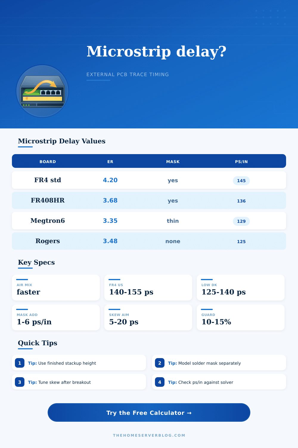
| 1 oz FR-4 top microstrip with mask | 5 to 8 mil | 4 to 7 mil | 3.8 to 4.4 | 140 to 155 ps/in |
| Low-Dk high speed top layer | 5 to 7 mil | 4 to 6 mil | 3.2 to 3.7 | 128 to 142 ps/in |
| RF laminate exposed microstrip | 8 to 18 mil | 6 to 12 mil | 3.0 to 3.6 | 118 to 134 ps/in |
| Fine pitch breakout microstrip | 3 to 5 mil | 3 to 5 mil | 3.6 to 4.2 | 138 to 152 ps/in |
| Polyimide flex microstrip | 3 to 8 mil | 2 to 5 mil | 3.2 to 3.6 | 126 to 142 ps/in |
| Solder mask condition | Field effect | Delay impact | When to use it | Layout note |
|---|---|---|---|---|
| No solder mask | More air field | Fastest external trace | RF coupon, exposed trace | Confirm finish and oxidation risk |
| Mask opening near trace | Partial air field | Small added delay | Pad escape, RF keepout | Model exact mask clearance |
| Thin mask over trace | Light dielectric loading | About 1 to 3 ps/in | Controlled process boards | Ask fabricator for mask thickness |
| Normal mask over trace | Moderate dielectric loading | About 2 to 6 ps/in | Common digital routing | Use solver for tight interfaces |
| Heavy mask or ink | More field in mask | Can exceed 6 ps/in | Labels, thick coatings | Avoid over timing-critical traces |
| Timing scenario | Delay item to budget | Common target | Calculator field | Practical review |
|---|---|---|---|---|
| DDR address and command | Group flight time and skew | Few ps to tens of ps | Timing budget and skew budget | Compare against controller layout rules |
| PCIe reference clock pair | P/N mismatch | Single-digit ps when possible | Differential length mismatch | Route symmetrically after breakout |
| MIPI or LVDS pair | Pair skew and lane skew | Interface-specific | Skew budget | Use actual package and connector data |
| Clock fanout tree | Trace delay matching | Endpoint dependent | Routed length and guard | Include buffer and via delays |
| RF microstrip phase | Electrical length | Frequency dependent | ps/in and ps/mm | Use EM solver for phase-critical work |
| Formula step | What it estimates | Primary inputs | Output | Limitation |
|---|---|---|---|---|
| Quasi-static microstrip Er | Effective dielectric constant | Trace width, height, board Er | Effective Er | Not a full field solver |
| Mask loading correction | Air field replaced by mask | Mask Er, thickness, coverage | Extra effective Er | Mask geometry is simplified |
| Velocity conversion | Signal speed along trace | Effective Er | in/ns and ps/in | Frequency dispersion omitted |
| Mismatch skew | Differential timing delta | Length delta, width delta | ps skew | Coupling effects approximated |
| Budget comparison | Remaining timing room | Trace delay, vias, guard | ps margin | Silicon timing must be added separately |
In low-speed digital logic, copper trace acts like just another wire. At high frequency it behaves as a transmission line with odd properties. Treated as a fixed connection between two points, it’s not. View it instead as a path with physics to consider.
Once you push into high-frequency signaling, the signal velocity is determined by electric field surrounding the copper. That’s when microstrip propagation delay comes into play. Rule-of-thumb values is usually wrong guesses, causing you to violate your timing. That’s where the effective dielectric constant comes into play. It’s at the heart of everything.
Why Copper Traces Are Not Simple Wires
On a PCB, a microstrip trace exist as an outer layer. Half the electric field are in the air and the other half is in the fiberglass board material. Since air has a dielectric constant of one and standard FR-4 is ~four, your signal sees a blend off both materials. That produces an effective value that governs velocity. If you ignore this split-field feature, delay estimations will be inaccurate by 10% or more.
To complicate things further there’s solder mask. That green epoxy covering the traces does protect them. However, it also loads the trace with more dielectric where there was air before. Even a typical amount of coverage plus its thickness will slow down your signal some so the tool models that as well. A few picosecs/inch add up quick when you’re working on narrow timing budgets.
There is no single generic delay number you can pull out of the datasheet and expect it’ll be applicable to your particular stackup. Every board vary by a little bit due to fabrication tolerances. The other design hazard is skew. You want your differential pairs to reach the end of the line together. If one trace are longer then the other, or if the trace width varies due to copper etching process, you create a timing mismatch. How much? That’s where the calculator comes in to help measure that with width variation and length difference.
It may look like routing symmetrical enough will do, but more often than not it doesn’t. Just the variation in copper plating alone can push delay over the margin of compliance in high speed interfaces such as PCIe or DDR.
Looking at the page’s reference table will show performance of various laminates. Lower Dk materials such as Rogers or Megtron tend to run faster due to reduced dielectric loading. You can achieve greater data rates without resorting to fancy balancing methods. However standard FR-4 do have its limitations and often times swapping out the material is a better solution rather than shrinking down trace geometry. Reducing geometry brings with it manufacturing risk which is hard to control.
Before routing, check those numbers against your timing budget for real world design. How many vias do you have? What’s their delay contribution? Are there still margins left if you account for component delays? The tool gives a guard band percentage so you can simulate conservative scenarios. Better to find during simulation that you’re short of margin rather than finding out during signal integrity testing after the boards are built. Fixing skew in silicon or after fabrication should of been done earlier because it is expensive and usually impossible.
The effect of temperature play a role in the propagation delay. Increasing the temperature will cause dielectric constants to shift ever so slightly. For example if your device gets hot it’ll have more delay. That’s why the calculator has a temperature adjustment. You want your timing to hold up when it’s under thermal stress and not just sitting on your benchtop at room temp. That’s what makes the difference between a working prototype and a robust product.
This is about managing propagation delay, i.e., managing expectations. This isn’t a magic trick; it’s working within the constraints of physics. What goes into the calculator are real physical parameters, such as mask coverage, copper thickness, dielectric height and trace width. These need to be reviewed from the actual stackup drawing, and you should talk to your fabricator to get them right. When you realize how these variables play out, then you stop guessing and begin to design with confidence. The signal arrives at the destination on time, every time.