Stripline Propagation Delay Calculator
Estimate internal PCB stripline velocity, one-way flight time, symmetric or asymmetric layer effects, differential pair skew, via delay, and remaining timing budget.
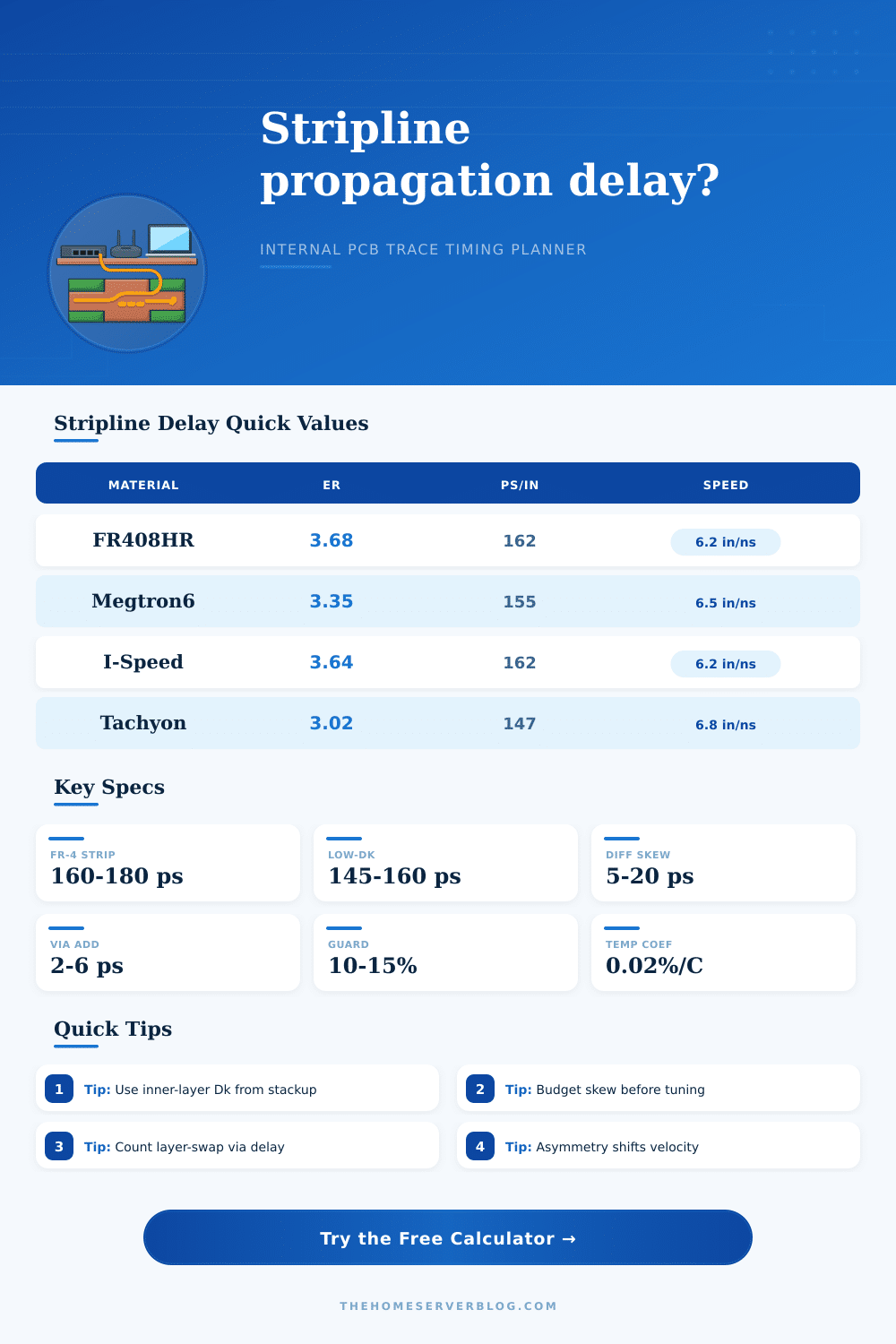
| Stripline material | Typical Dk | Approx ps/in | Best planning use |
|---|---|---|---|
| Isola FR408HR | 3.65 to 3.75 | 160 to 164 | Dense server boards, DDR routing, moderate-speed internal layers |
| Panasonic Megtron 6 | 3.35 to 3.55 | 155 to 160 | Long PCIe, Ethernet, and backplane-style differential pairs |
| Isola I-Speed | 3.60 to 3.70 | 160 to 163 | Cost-balanced high-speed stripline layers |
| Isola Tachyon 100G | 3.00 to 3.10 | 147 to 149 | Very high-speed SerDes with lower Dk and loss |
| Nelco N4000-13 SI | 3.55 to 3.75 | 159 to 164 | Signal-integrity controlled multilayers and telecom boards |
| Rogers RO3003 | 3.00 | 147 | RF-adjacent timing, clocks, and specialty controlled dielectric work |
| Structure | Plane spacing | Velocity behavior | Timing concern |
|---|---|---|---|
| Symmetric stripline | Top gap equals bottom gap | Most predictable, near full dielectric Dk | Usually best for matched clock, memory, and pair timing |
| Asymmetric stripline | One plane is closer | Slight Dk shift from field imbalance | Layer-to-layer swaps can create skew even with equal copper length |
| Symmetric differential stripline | Balanced cavity and pair field | Stable velocity with coupling correction | Use P/N mismatch plus breakout via delays for skew checks |
| Asymmetric differential stripline | Pair offset from cavity center | Slightly altered delay and impedance | Common in dense HDI boards where planes are not equally spaced |
| Dual stripline cavity | Two buried signal layers between planes | Layer choice may change delay | Check each layer separately before length matching between layers |
| Interface | Common stripline use | Skew target | Calculator check |
|---|---|---|---|
| DDR4 / DDR5 | Inner byte lanes and address buses | 10 to 25 ps | Compare DQ, DQS, address, and command groups against budget |
| PCIe Gen4 / Gen5 | Buried low-crosstalk differential pairs | 5 to 15 ps | Check P/N mismatch, via transitions, and layer changes |
| 10G / 25G Ethernet | Switch ASIC to cage or retimer | 5 to 20 ps | Estimate pair skew before final channel simulation |
| Clock distribution | Internal clock spine and fanout | By jitter budget | Convert trace length to flight time and reserve guard band |
| ADC / JESD links | Converter clock and serialized lanes | 5 to 30 ps | Screen route length balance and dielectric stackup impact |
| Formula item | Planning expression | What it means | When to refine |
|---|---|---|---|
| Velocity factor | 1 / sqrt(Dk eff) | Fraction of vacuum speed for buried trace | Always refine with stackup solver for signoff |
| Delay density | 84.7 x sqrt(Dk eff) | Approximate picoseconds per inch | Use field-solver value for impedance-controlled boards |
| Asymmetry factor | Abs(top - bottom) / average | How far the trace is from a centered stripline cavity | Important when matched nets change inner layers |
| Via contribution | Via count x ps per via | Transition and stub planning delay | Backdrill, model, or simulate high-speed vias |
| Skew from mismatch | Mismatch x ps per length | Delay difference from unequal copper length | Add package, connector, and layer-swap differences |
In a high speed design, signal propagation delay is frequentlly ignored as some minor nuisance, something solved at the last minute by length tuning software prior to fab. This completely overlooks the point. Deciding what direction your traces takes across the board stackup is where heavy lifting occurs.
If you route using stripline, you are sending your signals between ground plane, burying them. Why do this? It provides better shielding from external noise and lower crosstalk relative to microstrip. There is a cost however: loss of visibility into field distribution. Also you become dependent upon dielectrics whose properties can vary more different than you might expect. Getting a handle on what’s going on in those hidden layers is not so much about remembering equations as understanding where you are realy spending your timing budget.
How Signal Delay Works in Circuit Boards
Plug in the properties of each layer and their thickness, then let the calculator do the math (above). No more guessing to translate from physical size to time domain numbers. It factors in the varying signal velocity. The velocity vary greatly depending on the effective dielectric constant of the material around copper. How close is the ground plane? Is it closer on one side or farther away?
The electric field will be equally balanced between conductor and return in an even stripline. This keeps the velocity factor stable and thus predictable. But if your stackup dictates you must use an asymmetric layout where one ground plane is closer than another… well, the effective Dk change a little. And the velocity factor does too. These changes often won’t become apparent until production line. The tool takes that asymmetry penalty into account as part of the calculation and displays just how much additional delay your imbalanced design create.
Why should you care? A few billionths of a second of unintended skew will wreck tight timing margins on high speed differential pair. That leads us to the material used. I’ve seen a lot of designers choose their material more for price than electrical properties. While cheap FR-4 may get the job done, its Dk variation is quite broad. Transitioning to a low-loss laminate such as Tachyon or Megtron 6 reduces this variability and decreases dielectric constant (which in turn means higher signal speeds). These trade-offs are clearly outlined in the reference table on the page, where it becomes clear that a lower Dk matches directly to fewer picoseconds per inch of trace length. This isn’t anything huge, but when you’re routing PCIe lanes or memory buses with long, equal-length runs, it can make a difference between having to tune serpentine routes for hours or not.
You don’t need your bottom layer dragging your timing back unexpectedly after spending all those hours dialing everything in. Another secret sink for your timing budget is via transitions. Anytime there’s a signal moving between striplines layers by passing through a via, you’ll see stub effects and other impedance discontinuities that increases the overall delay. This is something many people ignore which results in overly optimistic estimates that prove wrong in the real world.
If you account for these specific delays, you can gain a realistic picture of how long it takes signals to fly. Then you must ask yourself: Can my leftover timing margin swallow up worst case variations due to temperature shifts and manufacturing tolerance? Ten percent is a decent place to start with guard bands; however, some aggressive designs may demand more. Remember, it’s not enough to hit the spec on paper. It needs to function reliably out in the field. Those values will shift somewhat as thermal expansion/contraction occurs and materials age.
Designing for good signal integrity is as much about setting expectations ahead of time as it is laying down copper on glass. Anticipate delay and construct your stronger system. Pay attention to asymmetry and the effect of vias. Apply good dielectric values in the inner layers. Think picosecond first, not just because it makes sense but because it prevents days of debugging later. Mostly, it’s knowing what to expect when you measure things. You should of anticipated this sooner.