PCB Trace Length Propagation Delay Calculator
Convert target delay to routed trace length, estimate Dk-based propagation, compare matched pair skew, and reserve serpentine length inside a timing budget.
| Target delay | Trace length | With vias | Serpentine reserve |
|---|---|---|---|
| 100 ps | 0.69 in | 108 ps | 0.07 in |
| 250 ps | 1.72 in | 258 ps | 0.17 in |
| 500 ps | 3.44 in | 508 ps | 0.34 in |
| 1000 ps | 6.88 in | 1008 ps | 0.69 in |
| Trace geometry | Typical effective Dk | Typical delay | Length matching use |
|---|---|---|---|
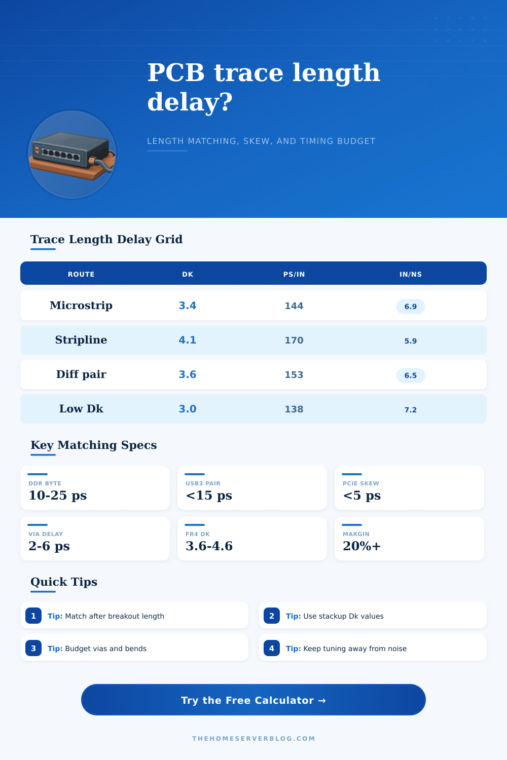
| Outer-layer microstrip | About 60% to 75% of Dk | 135 to 155 ps/in | DDR, clocks, general buses |
| Inner-layer stripline | Close to full Dk | 160 to 185 ps/in | Tight impedance and low EMI |
| Edge-coupled differential microstrip | Slightly above single microstrip | 145 to 165 ps/in | USB, LVDS, HDMI, MIPI |
| Differential stripline | Close to full Dk | 165 to 190 ps/in | PCIe, SerDes, dense routing |
| Low-Dk controlled route | Material dependent | 125 to 145 ps/in | Long high-speed channels |
| Interface | Common target | Skew focus | Layout reminder |
|---|---|---|---|
| DDR4 byte lane | Within 10 to 25 ps | Data to strobe | Match after package escape. |
| PCIe Gen4 pair | Under 5 ps intra-pair | P and N pair skew | Minimize asymmetry and vias. |
| USB 3.x pair | Under 15 ps intra-pair | Differential pair | Keep pair spacing consistent. |
| RGMII clock/data | Board skew plus clock mode | Clock to data | Account for PHY internal delay. |
| LVDS display | Pair-to-pair within UI margin | Lane group skew | Tune lanes in the same region. |
| Budget item | Typical value | Why it matters | Practical action |
|---|---|---|---|
| Serpentine reserve | 5% to 20% of route | Controls how much length can be added cleanly. | Reserve tuning room before placement locks. |
| Via delay | 2 to 6 ps each | Vias add delay and may create asymmetry. | Keep pair via counts equal. |
| Glass weave and Dk tolerance | Several ps/in spread | Real boards vary from nominal Dk. | Leave timing margin, especially on long traces. |
| Bend and meander coupling | Layout dependent | Tight meanders can self-couple and reduce added delay. | Use open spacing for tuning loops. |
Before laying down copper on a board, you can plug in your desired timing target to see what kind of skew allowance and trace length you’ll get from calculator. It converts something that’s a guessing game with no direction into a plan that can be executed predictably. From electrical time, youre now looking at physical distance, except remember: one inch of stripline isn’t the same as one inch of microstrip. That dielectric constant gets into it.
Trace length matching is actualy a material science challenge part of electromagnetic theory, but most designer think of it as a straightforward geometry issue. Your choice of route type in tool indicates to the system whether your signal will travel through air or more dielectric (i.e., epoxy and glass weave) on a given layer of your FR4 substrate. A one inch long trace running on layer 1 with some of its field energy in air will propagate faster then a one inch long trace buried totally in dielectric on layer four. These traces looks the same on screen, but the latter has much greater delay. Most unexplained timing issues stem from this difference.
How to Manage Timing in PCB Design
To handle such variations, the calculator includes them in calculation by calculating effective velocity according to the selected Dk value and geometry. Vias adds delay (typically two to six picoseconds per via) because parasitic inductance and capacitance slow down the signal transition. Therefore, you must treat your timing budget as a limited resource that is consumed by more than just straight lines.
For example, if you use a via on one side but not both sides of a differential pair, you’ve created skew which can’t be perfectly addressed with length tuning without creating impedance discontinuities. Before you even route anything, the tool allow you to enter number of vias you intend to use along with an estimate of how many picoseconds/via, so that you know immediately how much of your budget has been consumed. It makes you realize that all transitions from layer-to-layer cost you time.
Now we come to final option for the speedy designer: Serpentine tuning. This should always be last resort. On one hand, meandering introduces trace length (and therefore more inductance), which isn’t ideal. But on the other, it introduce inductance and has potential to create self-coupling at extremely close turns.
The winding allowance field in the calculator provides some leeway so that you can account for reasonable tuning real estate while placing routes. Five percent might be as much as you can accommodate given your channel density, less than that would mean squeezing in more turn than you have clearance space for. Better to over-estimate your routing room at place time then to discover youre out-of-space halfway through netlist routing.
Matching from package pins isn’t the real trick, though, matching from electrical endpoints is. Before even getting onto your controlled-impedance trace on-board, there’s delay inside the IC package, across the bond wires and out into the breakout region. Anything you do by trying to precisely match lengths on PCB is wasted effort if you ignore asymmetry of those source/load connections.
Standards such as PCIe or DDR4 has very specific, and sometimes very tight, intra-pair skew requirements. Hence their interface “presets”. Your USB 3 pair may be able to tolerate fifteen picoseconds of mismatch, whereas your PCIe Gen4 link may require fewer than five. Half the battle is knowing what budget applies to your design.
Another “hidden” variable that hammers high speed routing on conventional FR4 is glass weave shift. The Dk changes locally as you route across edge of two adjacent glass fiber orientations, which alters the speed locally. That introduces unpredictable skew that varies based off how laminate was constructed by each manufacturer and can’t be predicted perfectly by any calculator. So there’s no negotiating on the need for timing margin.
You can’t get all the way to your spec and hope it will come back to you reliably in production. In the end, it’s all about managing your uncertainty. The math’s taken care of by the calculator; you get to work out the trade-offs between signal integrity and layout density. It establishes a baseline for you, but ultimatelty it’s up to you to decide if that baseline works when moving from layout to chip.
By planning for via delays and leaving room for serpentine traces early on, you avoid the panic of having to tune lengths at last minute. Remember, this isn’t about reaching a number; rather, it’s about creating a strong link that functions in spite of the physical limitations imposed by the materials you’re working with. Make sure your traces remains straight, your pairs is symmetric, and your margins stay healthy, and the signals will find their way.