PCB Propagation Delay Calculator
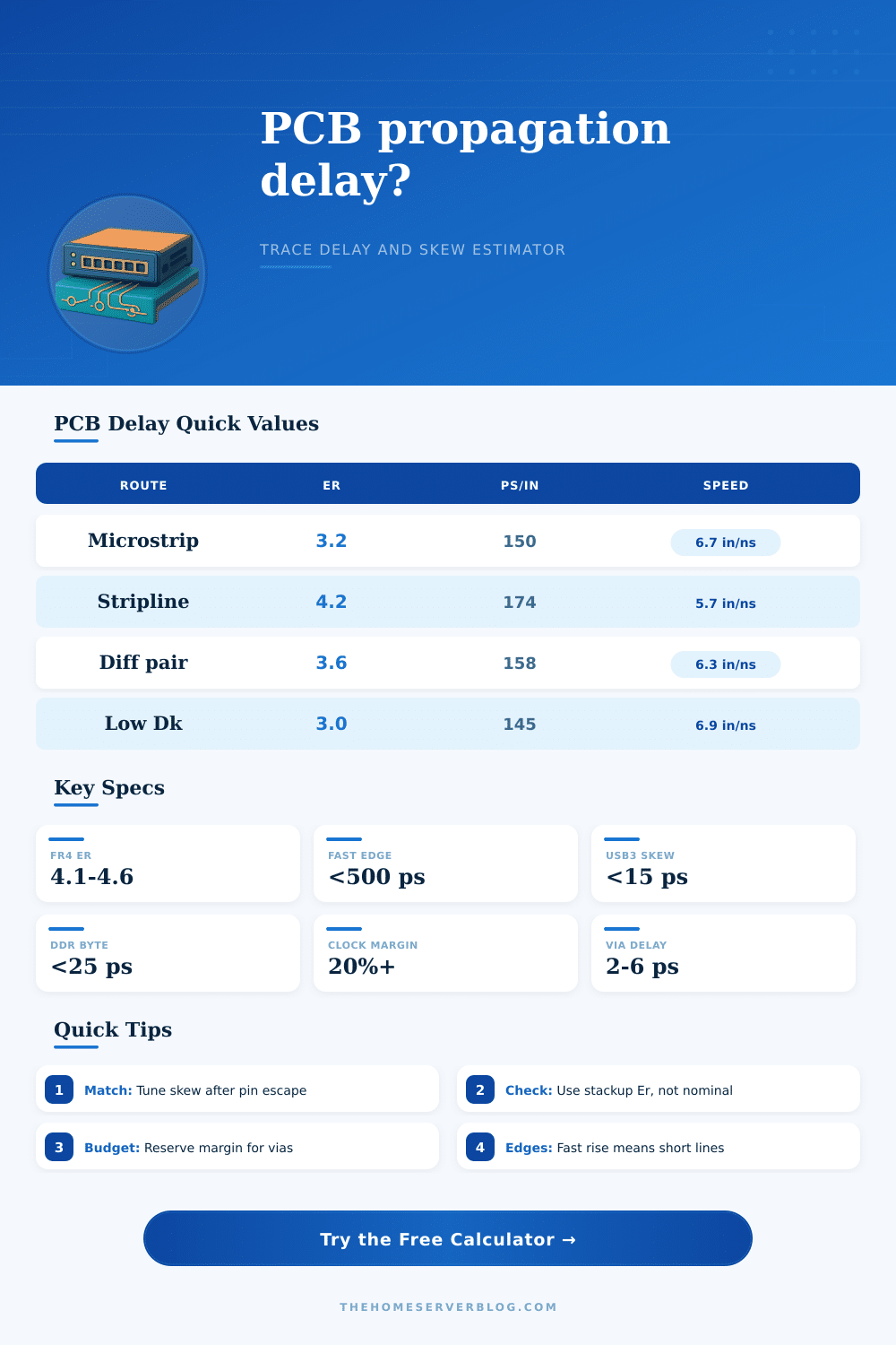
Estimate trace delay, signal velocity, differential pair skew, rise-time critical length, and timing margin for microstrip and stripline board routes.
| Laminate | Typical Er | Loss tangent | Where it helps |
|---|---|---|---|
| Standard FR-4 | 4.1 to 4.6 | 0.018 to 0.025 | General digital boards, short buses, low-cost prototypes |
| High-Tg FR-4 | 4.0 to 4.4 | 0.014 to 0.020 | Dense server boards and reflow-tolerant multilayers |
| Megtron 6 | 3.3 to 3.7 | 0.002 to 0.004 | PCIe, 25G links, long backplane-style routing |
| Rogers 4350B | 3.48 | 0.0037 | RF, clock distribution, controlled low-Dk work |
| Polyimide flex | 3.2 to 3.6 | 0.006 to 0.012 | Flex tails, cameras, compact board-to-board links |
| Geometry mode | Effective Er model | Delay behavior | Practical note |
|---|---|---|---|
| Outer microstrip | Air plus dielectric | Fastest common PCB route | More exposed to solder mask and weave variation |
| Embedded microstrip | Mostly dielectric | Between microstrip and stripline | Useful when the outer trace is covered or coated |
| Symmetric stripline | Close to Er | Slower, more predictable | Best for stable impedance and crosstalk control |
| Differential microstrip | Microstrip with coupling adjust | Slightly slower than single-ended | Spacing, solder mask, and reference gaps matter |
| Differential stripline | Stripline with coupling adjust | Stable but usually slowest | Common for high-speed internal pairs |
| Interface scenario | Typical concern | Starting skew target | Calculator use |
|---|---|---|---|
| DDR data byte lane | DQ to DQS timing window | 10 to 25 ps | Compare bus members and add margin for vias |
| PCIe or USB pair | P/N intra-pair skew | 5 to 15 ps | Check mismatch after breakout and AC caps |
| RGMII or RMII clock | Clock-to-data relationship | 50 to 500 ps | Estimate intentional clock delay or board skew |
| FPGA LVDS | Lane-to-lane alignment | 10 to 50 ps | Screen whether deskew logic has enough range |
| Backplane connector | Long route flight time | By protocol budget | Combine board trace, vias, and connector allowance |
| Rule of thumb | Formula | Meaning | Why it matters |
|---|---|---|---|
| Velocity factor | 1 / sqrt(Er eff) | Fraction of light speed in route | Turns material and geometry into speed |
| Delay density | 84.7 x sqrt(Er eff) | Approximate ps per inch | Fast way to compare stackups |
| Critical length | Rise distance / 6 | When trace acts like a transmission line | Flags routes needing impedance control |
| Skew from length | Mismatch x ps per length | Delay delta between matched routes | Checks tuning against interface budgets |
| Guard band | Delay x buffer percent | Reserve for uncertainty | Protects timing from stackup tolerance |
Signal timing problems is one of the biggest issues you face in high-speed PCB design. Your clock shows up late. Your data bus doesn’t arrive at all. This happens even though everything looks great on paper with straight traces and matched impedance.
The problem is likely due to propagation delay, specifically, electromagnetic waves that move slower as they pass through the dielectric material surrounding the copper traces. To get an idea of what’s causing the delay you don’t need to memorize equations. Understanding how your board stackup impact timing budgets will be enough. If you enter your routing parameters into the calculator above, it will do the math for you. It translates properties of the material into concrete picoseconds, so you can know precisely how long it takes a signal to cross a trace.
Why Signals Are Slow on Your PCB
That’s important because different geometries of the trace create different interactions between air and the dielectric. Stripline routes is sandwiched between ground planes, providing better shielding from external noise. These types of route take longer to propagate. Microstrip traces use just one reference plane (outer layers) and part of electric field exists in the air. Because air has a low dielectric constant, those same signals travel faster then if they were completely encapsulated in resin. Depending on type of laminate and the routing mode you choose, the calculator change the effective dielectric constant to match.
Many designers oversimplify the issue here: FR-4 isn’t one material; it’s a class of glass-reinforced epoxy composites whose properties depends on resin system, manufacturer, and even batch number. The variation from lot-to-lot can be on the order of ten percent for effective dielectric constant. Because a difference in permittivity translates into a change in velocity factor, it also affect propagation delay. If you match traces based off standard values but use a board material with a higher dielectric constant; due to temperature or moisture, for example, signals will reach their destinations at different times.
The chart above shows some common laminate types along with their typical values of permittivity (Dk) and loss tangent (tan delta). You’ll notice that high-speed designs typically employ low-Dk substrates such as Rogers or Megtron for critical nets. Low-Dk materials mean less uncertainty in calculated delays because they offer tighter control over the dielectric constant.
The other thing that is often overlooked until it blows up is rise time. A rapid rise time corresponds to a sharp edge on the signal, which in turn carries high frequency harmonics. The dielectric material has an effective dielectric constant at high frequencies that deviate from its DC value. Faster signals experience increasing dispersive effects. When designing your board, you can specify the expected rise time for your edges, and the calculator will tell you what’s called critical length. This is how long your trace should of be before transmission line effects start dominating the action. Under this length, a trace behaves mostly like a lumped capacitor. Above this length, the delay and reflections takes over.
Knowing this limit gives you guidance about when it really matters to match impedances. If your traces are short compared to rise time then you may not need such strict lengths or tight tolerances on geometry. Relax constraints where they don’t matter, and apply rigor where it does.
For differential pairs, skew between each pair must be tightly controlled, otherwise your common-mode rejection goes out the window. For single-ended buses such as DDR, lanes needs to be aligned with respect to bytes so they’re sampling the data at the right time within the clock window. The tool will estimate the skew based on the physical length mismatch and then include via delays.
Via delays can be small contributions that accumulate over longer routes. A via changes impedance. It creates a very short stub of a few picoseconds. This adds a few picoseconds of delay. There are dozens of vias on an escape from a backplane connector. Those few picoseconds accumulate into tens of picoseconds of skew. That’s something you budget for upfront so you don’t need to do a redesign later.
Time is the propagation delay. That’s right: it’s time… Specifically, time for your signal to travel along the length of your board via epoxy resin and glass fibers. Time is a finite resource; treat it as such and you’re able to harness high speeds. Why? Because there’s no way to get rid of it.
The point isn’t to get rid of delay, it’s to accurately predict it so that your design fits within your available timing budget. When you know what materials do to signals, you’re not guessing anymore. You’re designing on purpose. That’s the difference between a board that works on the bench and one that works reliably in the field, it’s about planning ahead instead of fixing mistakes after they happen.