Skin Depth Calculator
Estimate RF current penetration, useful conductor thickness, AC resistance ratio, and run loss for common home lab conductors.
Calculated RF conductor result
| Use case | Frequency | Copper depth | Five depths |
|---|---|---|---|
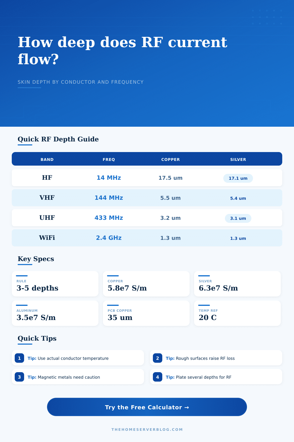
| AM broadcast wiring | 1 MHz | 66.1 µm | 330 µm |
| HF antenna feed hardware | 14 MHz | 17.7 µm | 88 µm |
| 2 meter VHF workbench | 144 MHz | 5.5 µm | 28 µm |
| 433 MHz telemetry | 433 MHz | 3.2 µm | 16 µm |
| 2.4 GHz WiFi layout | 2.4 GHz | 1.35 µm | 6.7 µm |
| 5 GHz WiFi layout | 5.8 GHz | 0.87 µm | 4.4 µm |
| Material | Conductivity | Relative µ | RF note |
|---|---|---|---|
| Silver | 63.0 MS/m | 1.0 | Best common surface conductor |
| Copper | 58.0 MS/m | 1.0 | Default PCB and cable reference |
| Aluminum | 35.0 MS/m | 1.0 | Needs oxide and joint attention |
| Brass | 15.9 MS/m | 1.0 | Common in connectors, higher loss |
| Nickel | 14.3 MS/m | 100 | Barrier layers can be lossy at RF |
| Mild steel | 6.0 MS/m | 80 | Use measured data for final design |
| Geometry | Best input | Capacity limit | Practical use |
|---|---|---|---|
| Round wire | Diameter | Surface circumference | Antennas and center pins |
| Flat strip | Width and thickness | Both broad faces | Ground straps and bus bars |
| PCB trace | Trace width and copper weight | Etched surface roughness | Microstrip and RF routing |
| Braided shield | Equivalent braid width | Coverage and weave | Coax shields and pigtails |
| Foil sheet | Sheet thickness | Folded edge current | Enclosure liners and shields |
| Project | Typical frequency | Primary check | Secondary check |
|---|---|---|---|
| HF receiver ground strap | 7 to 30 MHz | Copper strap depth | Bond length loss |
| VHF coax jumper repair | 144 MHz | Shield surface depth | Braid roughness |
| IoT telemetry enclosure | 433 or 915 MHz | Foil shield thickness | Seam resistance |
| WiFi PCB antenna feed | 2.4 or 5.8 GHz | Trace copper use | Roughness loss |
| SMA connector plating | 1 to 6 GHz | Silver or gold surface | Nickel underplate |
Unless I’ve missed my guess, you’ve probably constructed a radio project that didn’t work out because the signal wasn’t strong enough. Even though all the numbers worked on paper. And more often than not it’s not about the gain and it’s not really about the frequency either.
The problem is: how thick was your copper? Electricity doesn’t flow across the full cross section of wire at high frequencies like it will with direct current. No, at high frequencies, the current tend to crowd itself up against surface. That’s called the skin effect.
What Is Skin Effect?
Not accounting for this can mean wasting money on over-engineering your conductors or losing them due to underbuilding. With those two items (material and frequency), plug them into the calculator. The rest is handled by the calculator. You don’t have to do any conversion or coefficient guesswork. But knowing how it works will help you design more effectively.
So what is “skin depth”? Skin depth is distance below surface where the current density has decreased to approximately thirty-seven percent. In other words, it’s not a solid barrier; there’s still some current below that, but it drops off quickly. There’s a general rule-of-thumb that says 3x the skin depth contain roughly ninety-five percent of the current. A safe bet is that five times the skin depth hold almost all the current. Any thicker than this and you’re adding bulk your radio waves aren’t going to use.
The material selection do matter but maybe more so for a different reason. Silver conducts better then copper, which conducts better than aluminum. At most radio frequencies, however, the skin depth of copper versus silver make no noticeable difference. So where does the silver plating make a big difference? It is not really about conductivity, but rather because it prevents oxidation.
In the table on that page, you’ll notice that nickel is an excellent barrier layer but is also magnetic. If your plating is thicker than what’s necessary then nickel can severely increase loss. And this is where folks commonly go astray. They believe as long as it’s conductive, any layer are fine. It isn’t. How easily magnetic fields pass through is important as well, particulerly with nickel and/or steel. The permeability can reduce the effective depth even more.
Another overlooked variable here is temperature. The hotter the copper gets, the greater its resistivity. Greater resistivity equate to a greater skin depth. A greater skin depth results in use of more of the conductor. This uses more of the conductor and increases the resistance overall. Not a big deal, but if you’re pushing a lot of power through it, it becomes one. The amp operates hot? That changes the skin depth. The AC resistance climbs. You have to consider both the ambient temperature when you took those first measurements and the operating temperature.
Another biggie on RF is the roughness of surface. Rougher surfaces cause greater loss and resistance because the current has to travel further along a more winding route (skin depth < roughness of surface). A polished silver plating are ideal. Even something as simple as an etched PCB trace or rough braided shield can add noticeable loss at gigahertz frequencies. Apply a roughness factor to account for it with the calculator.
Know your materials. Even though you might be using thicker braid, a smooth foil shield will outshine it. It depends off geometry. Skin effect happen on the circumference of a round wire. It also happens on both broad faces of a flat strip, bar, or buss. That’s why a wide, flat strap is often used for grounding in RF situations. It provides a big surface area for current to travel on. It has low resistance and covers a short distance. Again, it is the skin, not the core.
Notice the ratio between AC and DC resistance in the results. That’s how much power you’re wasting as heat. For an idea of how much that matters, notice the estimated dB loss along your path length. Is that negligible? Maybe you can get away with a cheaper (or even thinner) conductor. Is that high? Time to reconsider both your geometry and/or materials.
Simply make something that is thick enough for the frequency you’re working with, smooth, and conductive. After that, there are diminishing returns for chasing a little bit more conductivity or bulk. You should of accounted for this. That’s why it’s mostly a matter of knowing what you’re measuring.
This isn’t about going big. It’s about making the right part of the thing count. As a result, your signal improves.